
China Moneypro
Types of Uncooled Detectors for Handheld Thermal Imaging
Explore a technical analysis of VOx and a-Si uncooled detectors for handheld thermal imaging. Learn about pixel pitch, NETD, and integration for EO/IR systems.
The landscape of handheld thermal imaging has undergone a radical transformation driven by the evolution of uncooled infrared detectors. For system integrators and optoelectronics engineers, selecting the correct detector architecture is no longer just about resolution. It involves a sophisticated trade-off between thermal sensitivity, pixel pitch, power consumption, and manufacturing scalability. As handheld devices demand higher performance in smaller form factors, the choice between Vanadium Oxide (VOx) and Amorphous Silicon (a-Si) becomes a critical decision point for product success in industrial, security, and outdoor markets.
Key Takeaways
- VOx microbolometers represent the gold standard for thermal sensitivity with NETD often below 30mK.
- The transition from 17μm to 12μm pixel pitch enables significantly more compact optics without sacrificing field of view.
- Wafer Level Packaging (WLP) is the primary driver for cost reduction and mass-market adoption in handheld EO/IR systems.
- System integrators must balance the thermal time constant of the detector with the frame rate requirements of the application.
- Advanced digital processing is now integrated directly into the detector module to minimize the workload on the host processor.
Physics of Uncooled Thermal Sensing
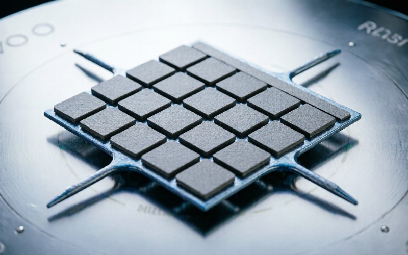
Uncooled detectors, or microbolometers, operate on the principle of change in electrical resistance when exposed to infrared radiation. Unlike cooled detectors that require cryogenic cooling to reach operational temperatures, uncooled FPAs (Focal Plane Arrays) operate at or near room temperature. This is achieved by suspending a thin membrane—the microbolometer—above the silicon read-out integrated circuit (ROIC) using thermal isolation legs. When infrared photons strike the membrane, its temperature rises, and the resulting change in resistance is measured by the ROIC.
The efficiency of this process is governed by the Temperature Coefficient of Resistance (TCR). A higher TCR means a larger change in resistance for a given change in temperature, leading to better sensitivity. Furthermore, the thermal mass of the membrane and the thermal conductance of the legs determine the thermal time constant, which impacts how quickly the detector responds to scene changes—a critical factor for handheld devices used in dynamic environments.
Vanadium Oxide VOx Detector Dominance
Vanadium Oxide remains the most widely utilized material for high-performance uncooled detectors. Its primary advantage lies in its high TCR and relatively low 1/f noise characteristics. For handheld thermal imaging systems where image clarity and long-range detection are paramount, VOx provides the necessary signal-to-noise ratio to achieve a Noise Equivalent Temperature Difference (NETD) of less than 30mK at f/1.0.
The manufacturing process for VOx is complex, involving the deposition of multiple phases of vanadium oxide to achieve the desired electrical properties. However, the industry has matured to the point where high-yield production is standard for resolutions ranging from 160×120 up to 1280×1024. For integrators, VOx offers a predictable roadmap for performance scaling, particularly in high-end handheld thermography tools and military-grade handheld EO/IR systems.
Amorphous Silicon a-Si Technology Attributes
Amorphous Silicon (a-Si) emerged as a strong competitor to VOx, primarily because it is a standard material in the semiconductor industry. This allows a-Si detectors to be manufactured in standard CMOS foundries, potentially lowering production costs. a-Si membranes are typically thinner and more uniform across the FPA compared to VOx, which can result in better image uniformity and fewer pixel defects.
However, a-Si generally exhibits lower TCR and higher 1/f noise than VOx. To compensate, a-Si detectors often require longer integration times or more aggressive signal processing, which can lead to higher power consumption or image lag. In handheld applications where low power and rapid response are critical, a-Si is often positioned for entry-level or mid-range devices where cost is the primary driver rather than absolute thermal sensitivity.
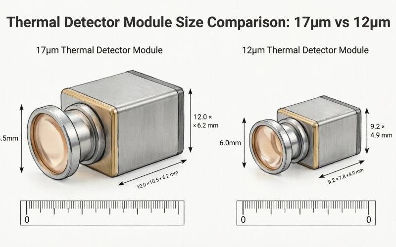
Impact of 12μm Pixel Pitch on Handheld Design
One of the most significant shifts in the last five years is the move from 17μm to 12μm pixel pitch. This reduction in pixel size has profound implications for the overall system design of handheld thermal imagers. A 12μm detector allows for a smaller FPA for the same resolution, which in turn reduces the diameter of the required optics.
For system integrators, this means the entire optical assembly can be made smaller and lighter, directly improving the ergonomics of handheld devices. Furthermore, the cost of germanium lenses—a major component of the bill of materials—is significantly reduced because smaller lens elements are required to cover the smaller image circle. This transition has enabled the creation of ultra-compact thermal modules that can be integrated into smartphones or ruggedized handheld tools without adding significant bulk.
Technical Comparison of Uncooled Detector Materials
| Parameter | VOx (Vanadium Oxide) | a-Si (Amorphous Silicon) | Thermopile Arrays |
|---|---|---|---|
| TCR (%/K) | ~2.0 – 3.0 | ~2.0 – 2.8 | N/A (Seebeck Effect) |
| 1/f Noise | Low | Moderate to High | Very Low |
| NETD (Typical) | <30mK to 50mK | 40mK to 70mK | >100mK |
| Pixel Pitch (Modern) | 12μm | 12μm – 17μm | >50μm |
| Thermal Stability | High | Moderate | Excellent |
Wafer Level Packaging and SWaP Optimization
Size, Weight, and Power (SWaP) are the defining constraints of handheld thermal imaging design. The advent of Wafer Level Packaging (WLP) has been a game-changer. Historically, microbolometers were sealed in bulky ceramic or metal vacuum packages with a sapphire or germanium window. WLP involves creating the vacuum seal at the wafer level before dicing, resulting in a package that is barely larger than the detector chip itself.
WLP not only reduces the physical footprint but also improves the thermal mass of the package, allowing for faster stabilization when the device is powered on. For integrators, WLP modules often come with integrated electronics that handle non-uniformity correction (NUC), bad pixel replacement (BPR), and even basic image enhancement. This “smart sensor” approach simplifies the integration process, allowing mechanical and software engineers to focus on the user interface and application-specific features.
Thermal Sensitivity and Image Processing Pipelines
In handheld applications, the raw data from the uncooled detector requires significant processing to be usable. Because uncooled sensors are sensitive to their own internal temperature changes, a temperature compensation algorithm is essential. Most high-quality handheld systems utilize a combination of internal temperature sensors and a mechanical shutter to periodically perform NUC. However, some advanced VOx modules now offer shutterless operation, using sophisticated algorithms to predict and subtract the thermal offset of the sensor itself.
The image processing pipeline also handles Detail Enhancement (DE) and Noise Reduction (NR). For system integrators, evaluating a detector’s raw sensitivity (NETD) is only half the battle; understanding how the module’s SDK handles these algorithms is equally important. A detector with an NETD of 40mK combined with superior image processing will often outperform a 30mK detector with a poorly optimized pipeline in real-world handheld scenarios.
Future Trends in Handheld Uncooled Systems
Looking ahead, the industry is pushing toward sub-10μm pixel pitches and the integration of multispectral capabilities. We are also seeing the rise of AI-on-the-edge, where deep learning models are integrated into the thermal module to perform automatic target recognition (ATR) or predictive maintenance diagnostics directly on the device. For handheld users in industrial settings, this means a thermal camera that doesn’t just show a hot spot, but identifies it as a specific failing component based on its thermal signature.
Furthermore, the push for lower power consumption continues. New ROIC architectures are being developed that utilize sub-threshold conduction and advanced power-gating techniques to extend the battery life of handheld devices from 4 hours to over 10 hours on a single charge. This is a critical requirement for emergency responders and utility inspectors who spend full shifts in the field.
What is the advantage of VOx over a-Si?
Vanadium Oxide (VOx) generally provides higher thermal sensitivity (lower NETD) and lower 1/f noise compared to Amorphous Silicon (a-Si). This results in clearer images with less graininess, making it the preferred choice for high-precision applications like long-range surveillance or detailed industrial thermography.
Why is 12μm pixel pitch becoming the standard?
The transition to 12μm allows for smaller detector chips, which reduces the size and cost of the required germanium optics. This is essential for creating truly portable, pocket-sized handheld thermal imagers and integrating thermal sensing into mobile devices without compromising on resolution.
What does NETD less than 30mK mean for the user?
Noise Equivalent Temperature Difference (NETD) is a measure of the sensor’s sensitivity. A value of less than 30mK means the detector can distinguish temperature differences as small as 0.03°C. This level of sensitivity is critical for identifying subtle thermal patterns, such as moisture intrusion in building walls or early-stage circuit board failures.