
China Moneypro
6 Types of Thermal Imager by Detectors
Discover the 6 types of thermal imagers and detector architectures. Learn how VOx, MCT, and T2SL impact SWaP-C for sensor integration engineers.
The six primary types of thermal imagers depend heavily on their focal plane array (FPA) architectures. Uncooled microbolometers (VOx, a-Si) dominate low-SWaP commercial applications, while cooled quantum detectors (InSb, MCT, T2SL, QWIP) provide the superior sensitivity and frame rates required for long-range, defense-grade electro-optical integrations.
Key Takeaways
- Vanadium Oxide (VOx) remains the industry standard for uncooled thermal imaging due to superior Temperature Coefficient of Resistance (TCR).
- Mercury Cadmium Telluride (MCT) offers unparalleled quantum efficiency but requires rigorous cryogenic cooling and non-uniformity correction (NUC).
- Type-II Superlattice (T2SL) detectors are rapidly replacing legacy MCT arrays, offering comparable performance with significantly higher array uniformity.
- Sensor integration engineers must balance SWaP-C (Size, Weight, Power, and Cost) constraints against Noise Equivalent Temperature Difference (NETD) requirements.
- Selecting the correct focal plane architecture directly dictates the read-out integrated circuit (ROIC) design and power budget.
As electro-optical and infrared (EO/IR) systems become increasingly advanced, sensor integration engineers face complex architectural decisions. Understanding the fundamental types of thermal imagers is no longer just about selecting an operational waveband; it requires a deep technical comprehension of focal plane array (FPA) physics, read-out integrated circuit (ROIC) interfacing, and cryogenic cooling constraints. This comprehensive engineering guide breaks down the six predominant infrared detector architectures, analyzing their physics, operational advantages, and integration trade-offs.
Uncooled Microbolometer
Uncooled thermal imagers dominate the high-volume infrared market. These thermal sensors operate at or near room temperature, eliminating the need for complex cryogenic coolers. Instead of relying on the photovoltaic or photoconductive effects, microbolometers absorb infrared radiation, which measurably alters the electrical resistance of the pixel material. Engineers must carefully evaluate the Temperature Coefficient of Resistance (TCR) and 1/f noise when integrating these sensors into low-SWaP (Size, Weight, and Power) platforms.
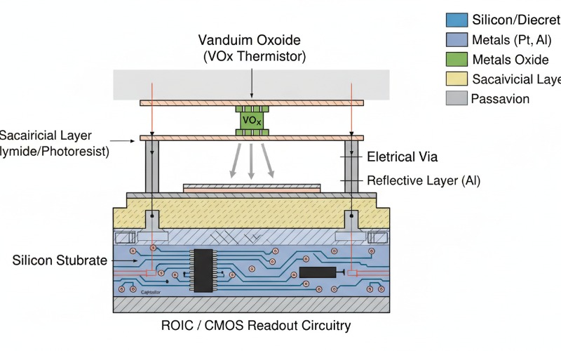
Vanadium Oxide (VOx) Detectors
Vanadium Oxide (VOx) represents the pinnacle of uncooled types of thermal imagers. This architecture relies on the distinct semiconductor-to-metal transition properties of vanadium dioxide. VOx arrays typically exhibit a TCR of roughly -2% to -3% per Kelvin, providing exceptional thermal sensitivity. Consequently, VOx FPAs can consistently achieve Noise Equivalent Temperature Differences (NETD) below 30 mK at f/1.0. Modern VOx pixel pitches have shrunk from 17µm down to 12µm and even 8µm. This miniaturization allows sensor integration engineers to design highly compact continuous zoom optics while maintaining high spatial resolution. Furthermore, VOx detectors require specialized thin-film deposition techniques, making them slightly more complex to manufacture than silicon alternatives, but the resulting thermal contrast and image stability are definitively superior for tactical military and high-end industrial applications. You can explore advanced uncooled integrations in our uncooled thermal core specification guide.
Amorphous Silicon (a-Si) Detectors
Amorphous Silicon (a-Si) is the secondary architecture in the uncooled domain. The primary engineering advantage of a-Si lies in its manufacturing compatibility. Because amorphous silicon processes align perfectly with standard CMOS foundry techniques, manufacturers can produce these thermal imagers at highly competitive price points. While a-Si detectors generally exhibit a slightly lower TCR and inherently higher 1/f noise compared to VOx, leading to higher NETD values (typically 40-50 mK), they offer exceptional uniformity across the array. Sensor integration engineers often select a-Si for commercial applications, such as automotive night vision and commercial fire-fighting thermography, where absolute radiometric precision takes a back seat to production scalability and ruggedness. Furthermore, a-Si arrays typically operate without the need for a strict thermoelectric cooler (TEC) for temperature stabilization, further reducing the overall power draw of the thermal module.
Cooled Quantum Detector
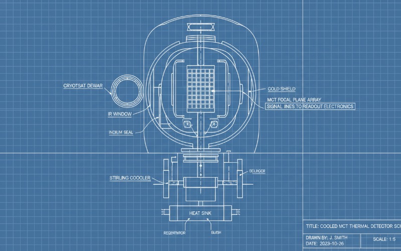
When integration scenarios demand extreme long-range target detection, rapid frame rates, or narrow-band spectral filtering, uncooled sensors become physically inadequate. Cooled quantum detectors absorb infrared photons directly, elevating electrons into the conduction band. Because thermally generated dark current would overwhelm this sensitive quantum interaction at room temperature, engineers must mate these sensors to mechanical cryocoolers (typically Stirling cycle engines) operating around 77 Kelvin. These architectures define the highest tier of the types of thermal imagers.
Indium Antimonide (InSb) Photodetectors
Indium Antimonide (InSb) is a direct bandgap semiconductor that has been the historical workhorse for Mid-Wave Infrared (MWIR) imaging. InSb FPAs are renowned for their near-perfect pixel operability and extraordinary spatial uniformity. Operating primarily in the 3 to 5 µm atmospheric transmission window, InSb detectors provide exceptionally high quantum efficiency (often exceeding 90%). For sensor integration engineers designing airborne gimbal payloads or naval fire control systems, InSb delivers crisp, high-contrast imagery even in high-humidity environments. However, InSb possesses a fixed bandgap. Therefore, it cannot be physically tuned for Long-Wave Infrared (LWIR) applications. Additionally, InSb requires stringent cooling, usually down to 77K or lower, which places heavy demands on the system’s cryogenic cooler and impacts the overall Mean Time To Failure (MTTF) of the electro-optical payload.
Mercury Cadmium Telluride (MCT / HgCdTe) Sensors
Mercury Cadmium Telluride (MCT) stands out as the most versatile, high-performance architecture among all types of thermal imagers. By precisely altering the ratio of mercury to cadmium during the epitaxial growth process, material scientists can tune the bandgap of the detector. This means MCT can be engineered to operate in the Short-Wave (SWIR), Mid-Wave (MWIR), or Long-Wave (LWIR) bands, and it even supports dual-band architectures on a single chip. MCT boasts exceptionally high quantum efficiency and low dark current, allowing for ultra-fast integration times necessary to track supersonic targets. However, the exact engineering challenge with MCT lies in its fragility and non-uniformity. The weak Hg-Te chemical bond makes the FPA susceptible to thermal stress, and the pixel-to-pixel uniformity is inherently lower than InSb. Consequently, integration engineers must implement rigorous two-point Non-Uniformity Correction (NUC) algorithms in the supporting video processing electronics. Read more about rigorous MCT calibration techniques to optimize your payload.
Type-II Superlattice (T2SL) Arrays
Type-II Superlattice (T2SL) architectures represent the modern evolution of high-performance thermal imaging. Engineered using alternating nanometer-scale layers of materials like Indium Arsenide (InAs) and Gallium Antimonide (GaSb), T2SL arrays create artificial bandgaps. This architecture successfully bridges the gap between the tunability of MCT and the uniformity of InSb. T2SL effectively suppresses Auger recombination rates, which significantly reduces dark current. From an integration standpoint, T2SL detectors can operate at slightly higher cryogenic temperatures (e.g., 90K – 110K for MWIR). This seemingly minor temperature increase drastically reduces the workload on the mechanical cryocooler, effectively extending the lifespan of the entire thermal imaging module. As a result, T2SL is rapidly displacing legacy MCT in new military acquisition programs. The Optica society routinely highlights T2SL as the foundational architecture for next-generation dual-band EO/IR systems.
Quantum Well Infrared Photodetectors (QWIP)
Quantum Well Infrared Photodetectors (QWIP) utilize Gallium Arsenide (GaAs) semiconductor technology. Unlike direct bandgap transitions, QWIP relies on intersubband transitions within the quantum wells. QWIP arrays are famous for their unparalleled pixel-to-pixel uniformity and exceptional array stability. They are strictly sensitive to the polarization of light and function exceptionally well in the LWIR band. However, QWIPs suffer from a major physical limitation: inherently low quantum efficiency (typically around 10-15%). To achieve an acceptable NETD, QWIPs require much longer integration times, making them unsuitable for tracking fast-moving targets. Sensor integration engineers typically deploy QWIPs in stationary, long-range scientific or ground-based observation systems where absolute image uniformity and low spatial noise are more critical than fast frame rates. Advanced documentation on QWIP uniformity is widely available through SPIE engineering publications.
Technical Specification Matrix: Detector Comparison
Understanding the exact specifications of these six types of thermal imagers is crucial for determining SWaP-C allocations. Below is an analytical matrix comparing standard engineering benchmarks.
| Architecture | Cooling Required | Primary Waveband | Quantum Efficiency | Uniformity | Cost Category |
|---|---|---|---|---|---|
| VOx (Vanadium Oxide) | Uncooled (Microbolometer) | LWIR | N/A (Thermal) | High | Low – Medium |
| a-Si (Amorphous Silicon) | Uncooled (Microbolometer) | LWIR | N/A (Thermal) | Very High | Very Low |
| InSb (Indium Antimonide) | Cryogenic (77K) | MWIR | Very High (>90%) | Very High | High |
| MCT (HgCdTe) | Cryogenic (77K) | SWIR / MWIR / LWIR | Very High (>80%) | Low | Very High |
| T2SL (Superlattice) | Cryogenic (90K – 110K) | MWIR / LWIR | High (~50-70%) | High | High |
| QWIP (Gallium Arsenide) | Cryogenic (70K) | LWIR | Low (10-15%) | Exceptional | Medium – High |
Engineering Deep-Dive: SWaP-C and Integration Trade-offs
In my 20 years of integrating EO/IR payloads for airborne and maritime applications, I have frequently witnessed the harsh realities of choosing the wrong detector architecture. During a recent project integrating an airborne intelligence, surveillance, and reconnaissance (ISR) gimbal, the initial design specified a legacy LWIR MCT detector. While the theoretical sensitivity was outstanding, the cryogenic cooler required to maintain the MCT array at 77K consumed an unacceptable portion of our power budget. Furthermore, the persistent vibrations from the rotorcraft caused constant drift in the MCT non-uniformity tables, requiring the operator to manually trigger the mechanical shutter for NUC every three minutes—an unacceptable distraction during tactical operations.
We pivoted the payload architecture to a modern MWIR T2SL detector. This transition allowed us to raise the focal plane operating temperature to roughly 105K. Consequently, the linear Stirling cooler drew substantially less current, solving our power budget crisis and significantly lowering the thermal signature of the gimbal housing itself. Because T2SL offers highly stable pixel uniformity, the requirement for mechanical shuttering was practically eliminated.
Conclusion
Selecting among the different types of thermal imagers dictates the entire trajectory of your optical, electronic, and software engineering efforts. Do not let outdated legacy datasheets dictate your next high-performance EO/IR payload. If you are struggling with SWaP constraints, cryocooler lifespan issues, or aggressive NUC requirements, you need a targeted engineering intervention. Download my Technical Maintenance and Architecture Checklist today, or schedule my Equipment Consultation to align your thermal imaging requirements with the cutting edge of focal plane technology.
People Also Ask (FAQ)
What are the two main types of thermal imagers?
The two primary categories are uncooled thermal imagers (using microbolometers like VOx or a-Si) and cooled thermal imagers (using quantum detectors like MCT, InSb, or T2SL). Uncooled imagers measure resistance changes from absorbed heat, whereas cooled imagers directly count infrared photons.
Why is VOx preferred over amorphous silicon in uncooled types of thermal imagers?
VOx (Vanadium Oxide) is preferred for high-end applications because it possesses a superior Temperature Coefficient of Resistance (TCR) and lower 1/f noise compared to amorphous silicon. This results in much higher thermal sensitivity, providing superior image contrast and a lower Noise Equivalent Temperature Difference (NETD).
How does T2SL compare to MCT in thermal sensor integration?
T2SL provides comparable bandgap tunability to MCT but benefits from stronger material bonds, higher pixel-to-pixel array uniformity, and lower Auger recombination rates. Because of these physics advantages, engineers can operate T2SL sensors at slightly higher cryogenic temperatures, reducing power draw and extending the cooler’s lifespan.
What is the primary disadvantage of QWIP thermal detectors?
The main disadvantage of QWIP (Quantum Well Infrared Photodetector) technology is its inherently low quantum efficiency, which typically hovers between 10% and 15%. Because it converts fewer incident photons into electrons, the system requires longer integration times, rendering QWIPs unsuitable for capturing rapid movement in dynamic tactical environments.