
China Moneypro
Thermal Imager NETD Sensitivity: The Ultimate Engineering Guide
Master thermal imager NETD sensitivity. Explore F-number impacts, pixel pitch limits, and VOx noise optimizations in EO/IR systems.
Noise Equivalent Temperature Difference (NETD) is the primary figure of merit for thermal imager sensitivity. It represents the minimal temperature difference an infrared sensor can resolve from background noise. In modern VOx uncooled microbolometers, state-of-the-art thermal imager NETD sensitivity operates sub-20mK at f/1.0, fundamentally dictated by pixel pitch, thermal time constant, and ROIC temporal noise.
Key Takeaways
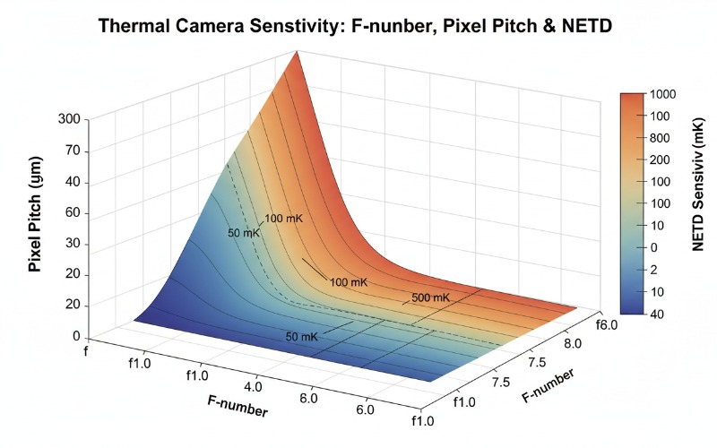
- Thermal imager NETD sensitivity is directly proportional to the square of the optical F-number.
- Scaling down pixel pitch (e.g., from 12µm to 8µm) exponentially increases the challenge of maintaining low NETD due to reduced pixel collection area.
- Vanadium Oxide (VOx) generally provides superior Temperature Coefficient of Resistance (TCR) compared to Amorphous Silicon (a-Si), yielding lower 1/f noise.
- ROIC architecture optimization, specifically capacitive transimpedance amplifier (CTIA) design, is critical for mitigating temporal noise in sub-20mK systems.
- Standardized NETD measurement requires rigorous control of blackbody differential temperatures and strict temporal noise variance calculations.
Fundamental Physics Governing Thermal Imager NETD Sensitivity
Understanding thermal imager NETD sensitivity requires a rigorous analysis of the underlying thermodynamic and electro-optical principles. The NETD equation encapsulates the holistic performance of the infrared detector system. Specifically, it correlates the detector noise voltage to the changing target temperature. Engineers calculate NETD using the ratio of total temporal noise voltage to the system responsivity relative to target temperature. Consequently, any optimization requires either reducing the intrinsic sensor noise or maximizing the thermal responsivity.
Total system noise is a root-sum-square synthesis of several independent noise mechanisms. First, Johnsen-Nyquist noise stems from the random thermal motion of charge carriers within the microbolometer resistor. Second, 1/f noise, or flicker noise, dominates at low frequencies and depends heavily on the bolometer material properties and bias parameters. Third, temperature fluctuation noise arises from the thermodynamic exchange between the suspended bolometer bridge and the underlying substrate. Therefore, improving thermal imager NETD sensitivity mandates a simultaneous suppression of these three primary noise sources while preserving the delicate thermal isolation of the micro-machined MEMS structure.
Impact of Pixel Pitch Scaling on Noise Equivalent Temperature Difference
The electro-optics industry continually drives toward reduced Size, Weight, Power, and Cost (SWaP-C). This trajectory heavily favors shrinking the microbolometer pixel pitch. We have transitioned from legacy 25µm and 17µm sensors down to modern 12µm, 10µm, and even 8µm architectures. However, reducing pixel pitch directly degrades thermal imager NETD sensitivity if all other variables remain constant. This degradation occurs because the radiometric energy collected by the pixel scales with the geometric area of the detector.
When an engineer shrinks a pixel from 17µm to 12µm, the active radiation-absorbing area drops by approximately 50 percent. Consequently, the signal-to-noise ratio plummets. To counteract this severe radiometric penalty, infrared sensor scientists must execute extreme innovations in MEMS fabrication. We increase the thermal isolation by thinning the structural support legs. Furthermore, we enhance the fill factor and optical absorption using advanced resonant cavity designs. These compensatory engineering feats ensure that modern 12µm uncooled microbolometers still achieve an exceptional NETD below 25mK.
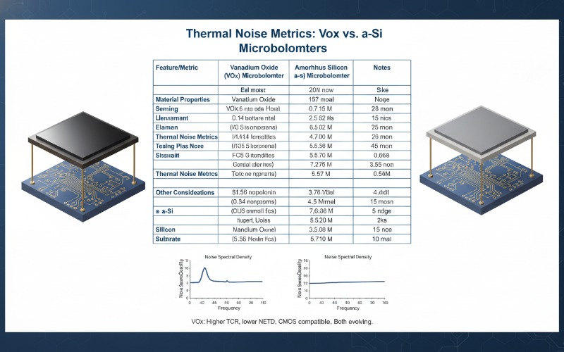
Microbolometer Material Dependencies: VOx vs. Amorphous Silicon
The active sensing material deposited on the MEMS bridge profoundly dictates the ultimate thermal imager NETD sensitivity. The two dominant commercial materials are Vanadium Oxide (VOx) and Amorphous Silicon (a-Si). Each material presents distinct optoelectronic advantages and manufacturing challenges. VOx has historically dominated the high-performance military and industrial sectors. Conversely, a-Si frequently finds utility in high-volume, cost-sensitive commercial applications due to its strict CMOS compatibility.
Vanadium Oxide offers a highly favorable Temperature Coefficient of Resistance (TCR), typically ranging from -2% to -3% per Kelvin. Furthermore, highly optimized VOx thin films exhibit substantially lower 1/f noise characteristics compared to standard a-Si layers. This superior signal-to-noise intrinsic baseline allows VOx sensors to achieve sub-20mK NETD values consistently. Alternatively, while a-Si presents slightly higher thermal time constants and higher 1/f noise profiles, modern manufacturing advancements continually narrow this performance gap. For absolute maximum thermal imager NETD sensitivity, VOx currently remains the definitive engineering standard.
| Technical Parameter | Vanadium Oxide (VOx) | Amorphous Silicon (a-Si) |
|---|---|---|
| Standard TCR (%/K) | -2.0 to -3.0 | -2.5 to -4.0 |
| 1/f Noise Magnitude | Low to Moderate | Moderate to High |
| Typical NETD (12µm, f/1.0) | < 20mK – 30mK | < 35mK – 50mK |
| Thermal Time Constant | 8ms – 12ms | 10ms – 16ms |
| CMOS Fab Compatibility | Specialized Equipment | Highly Compatible |
Engineering Deep-Dive: System-Level NETD Optimization Variables
Achieving ultra-low thermal imager NETD sensitivity requires a holistic system-level approach. Sensor scientists cannot merely rely on the focal plane array (FPA) to do all the heavy lifting. The optical assembly, readout electronics, and thermodynamic constraints must function in absolute unison. We categorize these system-level optimization variables into three distinct technical domains: optical throughput, temporal noise mitigation, and thermal responsiveness.
Optical F-Number and Radiometric Throughput
The optical F-number strictly defines the radiometric flux arriving at the focal plane array. Thermal imager NETD sensitivity degrades with the square of the F-number. For instance, transitioning from an f/1.0 lens to an f/1.4 lens cuts the incident infrared energy in half, thereby doubling the NETD value. High-performance thermal imaging modules utilize fast germanium or chalcogenide optics (e.g., f/1.0 or f/1.2) to maximize throughput. However, faster optics necessitate larger, heavier, and more expensive lens elements, directly conflicting with SWaP-C optimization goals. Engineers must critically balance optical speed against depth of field and system weight constraints.
Readout Integrated Circuit (ROIC) Noise Mitigation
The ROIC sits directly beneath the microbolometer array and translates microscopic resistance changes into multiplexed voltage signals. ROIC temporal noise severely limits thermal imager NETD sensitivity if poorly designed. Advanced ROIC architectures employ Capacitive Transimpedance Amplifiers (CTIA) to precisely integrate the minute signal currents. Furthermore, sophisticated skimming architectures strip away the massive background pedestal current, allowing the analog-to-digital converters (ADC) to utilize their full dynamic range strictly for the thermal differential signal. Precision bias voltage regulation ensures that self-heating effects do not saturate the integrators.
Thermal Time Constant vs. Sensitivity Trade-off
A critical engineering paradox exists between the thermal time constant and overall sensitivity. To achieve exceptional thermal imager NETD sensitivity, engineers increase the thermal isolation of the MEMS bridge, effectively decreasing thermal conductance (G). However, lowering G intrinsically increases the thermal time constant. If the time constant becomes too long (e.g., exceeding 15ms), the sensor exhibits severe motion blur or smearing when tracking fast-moving targets. Therefore, high-speed tactical systems deliberately sacrifice a few milli-Kelvins of NETD to maintain crisp temporal resolution under dynamic engagement scenarios.
First-Person Field Experience: Balancing NETD and Temporal Noise
In my 20 years designing integrated electro-optical (EO/IR) systems, I recall a highly specific airborne pod integration project. We were tasked with achieving a strict 25mK thermal imager NETD sensitivity using a new 10µm VOx core. During bench testing, the sensor easily met the 25mK specification. However, once integrated into the airborne gimbal, high-frequency vibration profiles coupled into the ROIC bias lines, introducing severe microphonic noise. The resulting temporal noise spiked the effective NETD to over 45mK in flight conditions.
To solve this, my engineering team had to perform a deep-dive redesign of the focal plane array bias regulation network. We implemented ultra-low-dropout (LDO) regulators precisely decoupled at the sensor socket, utilizing high-Q ceramic capacitors to filter out the mechanical resonance frequencies. Furthermore, we customized the non-uniformity correction (NUC) algorithms to run adaptive spatial noise filtering in real-time. By systematically eliminating the induced environmental noise, we successfully restored the intrinsic thermal imager NETD sensitivity to 24mK during live flight operations. This experience solidifies the reality that bench-level NETD means nothing if system-level integration is flawed.
Standardized Measurement Protocols for IR Sensor Scientists
Quantifying thermal imager NETD sensitivity demands rigorous adherence to standardized optoelectronic testing protocols. The methodology requires an extended-area cavity blackbody source characterized by absolute thermal stability. Typically, engineers capture multiple frames of data at two distinct background temperatures, usually 20°C and 35°C. The system computes the differential signal responsivity by subtracting the mean digital count values acquired at these two strict calibration points. This provides the crucial signal transfer function of the focal plane array.
Following responsivity calculation, the temporal noise must be precisely isolated. The test software captures a massive sequence of frames (often 64 or 128 frames) while staring at a uniform blackbody. The algorithm calculates the standard deviation of each individual pixel over time, effectively filtering out fixed pattern spatial noise. Finally, dividing the temporal standard deviation by the responsivity yields the precise NETD per pixel. According to standards published in the SPIE Digital Library, maintaining blackbody temperature stability within 0.001°C is absolutely vital for ensuring valid sub-20mK thermal imager NETD sensitivity validation.
Frequently Asked Questions
What is considered a good thermal imager NETD sensitivity rating?
For modern uncooled microbolometers, a high-performance thermal imager NETD sensitivity is generally considered anything below 30mK at f/1.0. State-of-the-art radiometric VOx sensors can achieve between 15mK and 20mK. Conversely, high-end cooled IR detectors (such as InSb or MCT architectures) routinely achieve NETD values well below 10mK due to cryogenic operation.
How does ambient temperature affect NETD measurements?
Ambient operational temperature drastically affects microbolometer responsivity. As the focal plane array substrate temperature fluctuates, the thermal conductance and baseline resistance shift. Uncooled systems without thermo-electric coolers (TEC-less architectures) utilize advanced ROIC compensation algorithms to maintain constant thermal imager NETD sensitivity across an operating range of -40°C to +85°C. Without this compensation, NETD degrades significantly at extreme temperature boundaries.
Why does 1/f noise limit ultra-low NETD achievements?
Flicker noise, or 1/f noise, exhibits increasing power density as operating frequency decreases. Because thermal imaging inherently involves staring at relatively slow-changing thermal scenes, the low-frequency domain dominates signal integration. Microbolometer materials intrinsically generate 1/f noise under electrical bias. If this noise floor is not suppressed via thin-film material optimization or ROIC chopping techniques, it fundamentally bottlenecks the ultimate achievable thermal imager NETD sensitivity.
Can software algorithms artificially improve NETD?
Software cannot alter the fundamental thermodynamic limits of the sensor element. However, advanced temporal and spatial noise filtering algorithms (such as 3D noise reduction) can drastically lower the apparent noise floor of the final video stream. While the raw analog thermal imager NETD sensitivity remains unchanged, the post-processed image displays a significantly higher signal-to-noise ratio, presenting a cleaner image to the human operator or edge-AI processor.
Concluding Thoughts on Infrared Sensitivity Optimization
Mastering thermal imager NETD sensitivity is the defining challenge for infrared sensor scientists and electro-optical engineers. The intricate balance between pixel pitch miniaturization, VOx material refinement, ROIC temporal noise mitigation, and optical throughput demands uncompromising precision. As autonomous targeting systems, thermography drones, and defense optoelectronics advance, the reliance on sub-20mK NETD sensors will continually escalate. My extensive background in field integrations proves that achieving optimal thermal imager NETD sensitivity is not merely an academic exercise; it is a critical operational necessity. Download my Electro-Optical System Maintenance Checklist today, or Schedule my Equipment Consultation to architect the perfect infrared integration strategy for your next mission-critical deployment.