
China Moneypro
What Is a Thermal Imager? Microbolometers Explained
Discover what a thermal imager is in this deep-dive on VOx microbolometers. Learn about NETD, ROIC architecture, and pixel pitch. Schedule a consult!
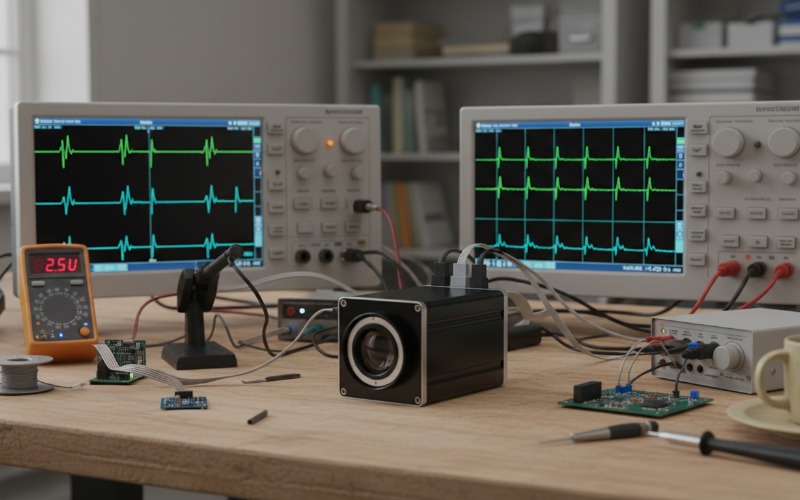
A thermal imager detects infrared radiation in the 8-14 µm wavelength band and translates microscopic temperature differences into a visible electronic video stream. Uncooled thermal imager microbolometers serve as the industry standard, utilizing micro-electro-mechanical systems (MEMS) and vanadium oxide (VOx) sensor arrays to measure resistance changes proportional to absorbed incident heat without requiring cryogenic cooling.
As optoelectronics engineers, we continually push the boundaries of infrared detection. For over two decades, I have designed integrated electro-optical (EO/IR) systems, and the most frequent question I receive from new engineers is fundamental: what is a thermal imager, and how do uncooled systems achieve such remarkable thermal sensitivity? The answer lies in the intricate physics and material science of thermal imager microbolometers. This guide provides a definitive engineering breakdown of microbolometer operation, material selection, and sensor integration to help you optimize your next infrared architecture.
Key Takeaways
- Uncooled thermal imager microbolometers predominantly operate in the Long-Wave Infrared (LWIR) atmospheric window (8-14 µm).
- Vanadium Oxide (VOx) detectors deliver superior Temperature Coefficient of Resistance (TCR) and lower 1/f noise compared to amorphous silicon (a-Si).
- Noise Equivalent Temperature Difference (NETD) and pixel pitch dictate absolute thermal sensitivity and spatial resolution limits.
- Read-Out Integrated Circuits (ROIC) utilize skimming circuits and capacitive transimpedance amplifiers to translate micro-Ohm resistance shifts into digital data.
How Does a Thermal Imager Work? Microbolometers Explained
At its core, a thermal imager is a highly specialized radiometric camera. Instead of capturing reflected visible light, it detects emitted thermal radiation. Every object with a temperature above absolute zero emits blackbody radiation. According to Wien’s Displacement Law, objects at terrestrial ambient temperatures emit peak radiation in the Long-Wave Infrared (LWIR) spectrum. To capture these photons, we rely on uncooled thermal imager microbolometers. Unlike older photon detectors that required heavy cryogenic coolers to suppress thermal noise, microbolometers function as thermal detectors operating at room temperature.
The Physics of Infrared Transduction
The fundamental unit of a thermal imager is the microbolometer pixel. Each pixel is an isolated microscopic thermistor suspended above a silicon substrate. We manufacture these pixels using advanced MEMS fabrication techniques. The pixel structure consists of a thin infrared-absorbing membrane suspended by two narrow thermal isolation legs. When LWIR photons pass through the optical assembly, they strike the membrane. The membrane absorbs the infrared energy, causing its physical temperature to rise slightly—often by just a few millikelvin. Because the membrane is thermally isolated by the legs, the heat cannot rapidly dissipate into the substrate beneath it.
Converting Heat to Resistance Shifts
This microscopic temperature increase triggers the true magic of the microbolometer: a measurable shift in electrical resistance. The membrane is coated with a thermally sensitive material characterized by a high Temperature Coefficient of Resistance (TCR). TCR defines the percentage change in resistance per degree Kelvin. When the membrane heats up, its electrical resistance drops. The underlying electronics send a precisely calibrated bias current through the thermal isolation legs and across the membrane. By measuring the voltage drop, the system calculates the exact resistance change. Consequently, this analog electrical signal accurately represents the incident infrared energy.
Material Science Determines Sensor Performance: VOx vs. Amorphous Silicon
When specifying infrared detectors for aerospace or industrial applications, you must choose between the two dominant thermistor materials: Vanadium Oxide (VOx) and Amorphous Silicon (a-Si). Both materials dominate the commercial landscape, but they possess fundamentally different semiconductor characteristics. Understanding these differences is critical for optimizing sensor performance.
| Technical Specification | Vanadium Oxide (VOx) | Amorphous Silicon (a-Si) |
|---|---|---|
| Temperature Coefficient of Resistance (TCR) | -2.0% to -3.0% / K | -1.0% to -2.5% / K |
| 1/f Electrical Noise | Significantly Lower (Superior) | Higher |
| Typical NETD (@ f/1.0 aperture) | < 30 mK | < 40 mK |
| Manufacturing Complexity | High (Requires specialized foundries) | Low (Standard CMOS compatible) |
| Primary Market Applications | High-End Military, Advanced Thermography | High-Volume Commercial, Automotive |
Vanadium Oxide (VOx) Detector Superiority
VOx is undeniably the gold standard for high-performance uncooled thermal imagers. Developed initially for classified military programs, VOx boasts an exceptional TCR, usually hovering around -2% to -3% per Kelvin. Furthermore, VOx exhibits remarkably low 1/f noise (flicker noise). Low noise floors are vital because the resistance changes induced by infrared absorption are incredibly small. A low noise floor allows the signal-to-noise ratio (SNR) to remain robust even when viewing low-contrast thermal scenes. The primary drawback of VOx is its complex fabrication. It is not inherently compatible with standard CMOS silicon foundries, necessitating specialized sputtering and annealing processes.
Amorphous Silicon (a-Si) Alternatives
Conversely, amorphous silicon provides a highly cost-effective alternative. Because a-Si is entirely compatible with standard CMOS semiconductor fabrication, manufacturers can scale production rapidly and reduce costs. However, a-Si typically exhibits a lower TCR and higher inherent 1/f noise than VOx. While algorithmic advancements have bridged the performance gap considerably, optoelectronics engineers generally prefer VOx when maximum thermal sensitivity and minimal noise equivalent temperature difference (NETD) are non-negotiable project requirements.
Navigating Read-Out Integrated Circuit (ROIC) Architecture
The thermistor membrane is only half of the equation. Directly beneath the MEMS structure lies the Read-Out Integrated Circuit. This complex silicon microchip serves as the bridge between the analog microbolometer and the digital processing pipeline. A modern ROIC architecture utilizes sophisticated Capacitive Transimpedance Amplifiers (CTIA) to accurately measure the tiny currents passing through the pixels.
One massive engineering challenge is the large baseline resistance of the microbolometer. The actual resistance change caused by a thermal target is merely a tiny fraction of a percent of the detector’s total baseline resistance. To prevent this massive DC background signal from overwhelming the amplifier and saturating the analog-to-digital converter (ADC), the ROIC employs active “skimming” circuits. These circuits mathematically subtract the baseline background current, allowing the amplifier to apply high gain strictly to the minute signal variations caused by the infrared scene.
Field Experience: Diagnosing ROIC Saturation in Drone Payloads
During a recent deployment integrating a 12 µm VOx thermal imager into a high-altitude UAV platform, my team encountered a severe ROIC saturation issue. We were tasked with monitoring an industrial flare stack. The core of the flare operated at extremely high temperatures, while the surrounding environment was a freezing winter landscape. The immense dynamic range of the scene exceeded our initial ROIC integration time settings. The excessive photon flux from the flare caused the active pixel capacitors to fill and saturate instantly, blinding the entire localized region of the array.
To resolve this, we reprogrammed the ROIC via its serial interface to implement a dynamic multi-integration time strategy. By interleaving short integration frames for the extreme hot spots and long integration frames for the cold background, we successfully preserved the high-fidelity radiometric data across the entire scene. If you are struggling with dynamic range limitations in harsh environments, I highly recommend consulting the SPIE Digital Library for advanced multi-integration algorithmic approaches.
Evaluating System Performance: NETD and Pixel Pitch
Two primary specifications define the capability of any microbolometer array: Noise Equivalent Temperature Difference (NETD) and pixel pitch. Engineers must balance these metrics carefully when designing customized LWIR optics assemblies.
Noise Equivalent Temperature Difference (NETD)
NETD represents the absolute smallest temperature difference that a thermal imager can resolve from the background noise. It is typically measured in millikelvin (mK). A lower NETD value denotes higher sensitivity. Today, high-end VOx detectors routinely achieve NETD values below 30 mK. However, NETD is highly dependent on the f-number of the optical lens used during measurement. An NETD of 30 mK at f/1.0 is drastically superior to an NETD of 30 mK at f/1.4. Always verify the optical aperture specifications when comparing manufacturer datasheets.
The Evolution of Pixel Pitch
Pixel pitch refers to the physical distance from the center of one microbolometer pixel to the center of an adjacent pixel. Historically, standard uncooled detectors featured a 17 µm pitch. Today, the industry has rapidly adopted 12 µm and is aggressively pushing toward 8 µm geometries. Smaller pixel pitches allow engineers to pack more pixels into a smaller silicon die, reducing the size, weight, and power (SWaP) footprint of the sensor. Moreover, smaller pixels allow the use of smaller, lighter, and less expensive germanium lenses.
However, physics demands a compromise. Reducing the pixel pitch decreases the physical surface area available to capture incoming infrared photons. Less surface area inherently means lower thermal sensitivity unless the MEMS design, thermal isolation legs, and ROIC noise floor are drastically improved to compensate. Advanced semiconductor nodes and enhanced umbrella structures have allowed 12 µm detectors to match the NETD performance of legacy 17 µm detectors, representing a monumental triumph in optoelectronics engineering.
Next Steps for Integrating Thermal Imager Microbolometers
Ultimately, engineering a flawless infrared system requires precise coordination between the detector array, the read-out electronics, and the optical lens. You must ensure rigorous flat-field correction (FFC) algorithms and bad pixel replacement strategies are continuously running to maintain image uniformity. If your deployment requires precise radiometric temperature measurement rather than qualitative imaging, leveraging professional calibration services is absolutely mandatory to correlate digital counts to absolute temperature metrics accurately.
Selecting the optimal thermal imager microbolometers dictates the success of your final product. From maximizing the VOx signal-to-noise ratio to preventing ROIC saturation in high dynamic range environments, engineering excellence is non-negotiable. If you need actionable guidance for your next system build, download my comprehensive Optical Engineering Maintenance Checklist, or schedule your custom Equipment Consultation today to guarantee your EO/IR architecture leads the market.
What is the difference between cooled and uncooled thermal imagers?
Cooled thermal imagers utilize integrated cryogenic coolers to lower the detector temperature drastically, reducing thermally induced electrical noise. They typically operate in the Mid-Wave Infrared (MWIR) band and offer extreme sensitivity and long-range detection. Uncooled thermal imagers utilize microbolometers operating at ambient room temperatures to detect Long-Wave Infrared (LWIR) radiation. They offer significant advantages in size, weight, power consumption, and long-term reliability due to the lack of moving mechanical cooler parts.
How does pixel pitch affect thermal imager microbolometers?
Pixel pitch determines the physical size of individual detectors within the array. A smaller pixel pitch (such as 12 µm or 8 µm) allows for higher resolution within the same physical footprint, or a smaller overall sensor size for the same resolution. This enables the use of smaller, less expensive optical lenses. However, shrinking the pixel reduces the photon-gathering surface area, which can negatively impact thermal sensitivity (NETD) unless advanced fabrication techniques and highly optimized ROIC architectures are employed to mitigate the signal loss.
What is NETD in thermal imaging?
Noise Equivalent Temperature Difference (NETD) is a critical performance metric expressing the smallest temperature difference a thermal imager can distinguish from background noise. Typically measured in millikelvin (mK), a lower NETD indicates a more sensitive detector. High sensitivity is crucial for resolving low-contrast objects, operating in poor weather conditions like heavy fog or rain, and ensuring accurate analytical thermography in industrial inspection applications.