
China Moneypro
What Is Electro-Optical (EO) Technology?
Deep dive into Electro-Optical (EO) technology. Explore EO/IR sensor mechanics, wavebands, and integration strategies for defense and industrial systems.
Key Takeaways regarding EO/IR Systems
- Definition: Electro-Optical (EO) technology bridges optics and electronics, converting photons into electronic signals for visualization, measurement, and tracking across the electromagnetic spectrum (UV to LWIR).
- Market Relevance: Critical for multi-sensor payloads in UAVs, border security, and industrial automation, where EO/IR fusion provides 24/7 situational awareness.
- Performance Metrics: Key integration parameters include Pixel Pitch (down to 10μm), NETD (<30mK), and SWaP-C (Size, Weight, Power, and Cost) optimization.
- Integration: Modern EO systems prioritize standard interfaces (MIPI, GigE) and robust SDKs to reduce development time for system integrators.
Defining Electro-Optical Technology in Modern Engineering
Electro-Optical (EO) technology is the branch of physics and engineering that encompasses the generation, detection, and manipulation of light (photons) and its conversion into electrical signals (electrons). For B2B system integrators and defense manufacturers, EO technology is rarely used in isolation; it is the foundation of complex EO/IR (Electro-Optical/Infrared) systems that combine visible light cameras with thermal imaging sensors to provide comprehensive environmental data.
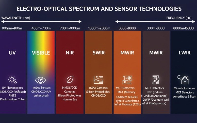
At its core, an EO system relies on a transducer—typically a Focal Plane Array (FPA)—to capture electromagnetic radiation. While “Electro-Optics” technically covers the entire optical spectrum, in practical industrial and defense applications, it specifically refers to systems operating within the Ultraviolet (UV), Visible (VIS), Near-Infrared (NIR), Short-Wave Infrared (SWIR), Mid-Wave Infrared (MWIR), and Long-Wave Infrared (LWIR) bands.
The Physics of EO Sensors: Photons to Electrons
Understanding the underlying physics is essential for selecting the correct sensor for specific integration requirements. The primary mechanism in EO sensors is the photoelectric effect (for photon detectors) or the bolometric effect (for thermal detectors).
Photon Detectors (VIS, NIR, SWIR, MWIR)
Photon detectors utilize semiconductor materials with specific bandgaps. When a photon with sufficient energy strikes the material, it excites an electron from the valence band to the conduction band, generating a measurable current. Common materials include:
- Silicon (Si): Used for Visible and NIR (up to ~1.1μm).
- Indium Gallium Arsenide (InGaAs): The standard for SWIR (0.9μm to 1.7μm), crucial for laser spot tracking and imaging through haze.
- Indium Antimonide (InSb) & Mercury Cadmium Telluride (MCT): High-performance cooled detectors for MWIR and LWIR, offering extreme sensitivity but requiring cryogenic cooling (Stirling coolers).
Thermal Detectors (LWIR)
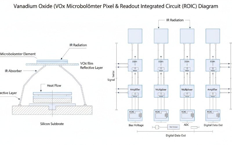
For Long-Wave Infrared (8-14μm), uncooled microbolometers are the industry standard for SWaP-constrained applications. These sensors do not count individual photons. Instead, they measure the change in resistance caused by the heating of the pixel element by incoming infrared radiation.
Vanadium Oxide (VOx) is the superior material for microbolometers compared to Amorphous Silicon (a-Si), offering higher Temperature Coefficient of Resistance (TCR) and lower noise patterns. This results in better NETD (Noise Equivalent Temperature Difference), often <30mK or <20mK in premium /infrared-detectors/.
Spectral Bands and Application Specifics
System integrators must match the spectral response of the EO sensor to the atmospheric conditions and target signature.
| Spectral Band | Wavelength | Primary Technology | Key Application |
|---|---|---|---|
| Visible (VIS) | 0.4 – 0.7 μm | CMOS / CCD | Daytime surveillance, color identification |
| Near-Infrared (NIR) | 0.7 – 1.1 μm | Low-Light CMOS | Night vision (intensified), license plate recognition |
| Short-Wave IR (SWIR) | 0.9 – 1.7 μm | InGaAs | Seeing through smoke/haze, laser designator imaging |
| Mid-Wave IR (MWIR) | 3 – 5 μm | Cooled MCT / InSb | Long-range coastal surveillance, missile seekers |
| Long-Wave IR (LWIR) | 8 – 14 μm | Uncooled VOx | Thermography, firefighting, drone payloads, security |
Critical Performance Metrics for Integrators
When sourcing EO modules or /thermal-cores/, generic resolution stats are insufficient. Engineering-grade evaluation requires analysis of the following:
1. NETD (Thermal Sensitivity)
Measured in millikelvins (mK), NETD represents the smallest temperature difference a sensor can distinguish from the noise floor. A lower NETD means a cleaner image with higher contrast. Modern VOx sensors achieve <30mK, which is critical for identifying targets in low-contrast environments (e.g., a person standing in front of a warm wall).
2. Pixel Pitch and SWaP-C
The industry has shifted from 17μm to 12μm and now 10μm pixel pitch standards. Smaller pixels allow for smaller focal length lenses to achieve the same operational range (Detection, Recognition, Identification – DRI). This reduction in glass size significantly lowers the weight and cost of the overall optical assembly, optimizing SWaP-C (Size, Weight, Power, and Cost) for UAV payloads and handheld devices.
3. Frame Rate and Latency
For dynamic applications like drone tracking or weapon sights, high frame rates (50Hz/60Hz) are non-negotiable to prevent image blurring. Furthermore, low-latency video output is essential for closing the loop in automated tracking systems.
Integration Challenges: Electrical and Software
Integrating an EO/IR module involves more than mechanical mounting. The data pipeline is critical for modern intelligent systems.
Video Interfaces
Legacy analog video (CVBS) is being replaced by high-speed digital interfaces necessary to carry 14-bit raw thermal data for radiometric processing:
- MIPI CSI-2: Preferred for embedded systems and drone SoCs (System on Chip).
- Camera Link: Standard for high-bandwidth industrial inspection.
- GigE Vision: Ideal for distributed networks and perimeter security /thermal-security-cameras/.
- USB 3.0: Common for lab analysis and plug-and-play modules.
Software Development Kits (SDK)
The hardware is only as good as the software driving it. Advanced EO modules come with comprehensive SDKs (Linux/Windows/Android) that allow access to Non-Uniformity Correction (NUC) tables, bad pixel replacement, and radiometric temperature data. For AI integrators, the ability to access raw digital counts before Automatic Gain Control (AGC) is applied is vital for training neural networks on thermal data.
The Future of EO Technology: Multi-Sensor Fusion
The frontier of Electro-Optical technology lies in Sensor Fusion. Single-modality sensors have limitations: visible cameras fail in darkness, and thermal cameras struggle with reading signage or glass surfaces. Fusion algorithms combine the high spatial resolution of visible CMOS sensors with the thermal contrast of LWIR sensors.
This results in an enhanced image where thermal signatures are overlaid with visible edge details, providing operators with unparalleled situational awareness. As edge computing power increases, we are seeing EO modules with built-in NPUs (Neural Processing Units) performing object detection and classification directly at the sensor level, reducing bandwidth requirements for transmission.
Frequently Asked Questions
What is the difference between EO and IR sensors?
Why is VOx preferred over a-Si for uncooled detectors?
What does “Cooled” vs “Uncooled” mean in EO technology?